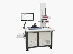
Professional Stylus Surface Profiler
A Professional Stylus Surface Profiler is a high-precision measurement instrument designed for accurate surface roughness and profile analysis of industrial components. The Professional Stylus Surface Profiler uses a diamond stylus sensor to trace micro-surface variations with exceptional resolution, converting physical surface texture into precise digital data. The Professional Stylus Surface Profiler is ideal for applications requiring strict surface quality evaluation and repeatable measurement accuracy in modern manufacturing environments.
- Measurement: Probe profiling technology
- Probe Sensor: Low inertia sensor (LIS3)
- Probe Pressure: Using LIS3 sensor: 1 to 15mg
- Sample View: Selectable magnification, 1 to 4mm FOV
Product Description
The Professional Stylus Surface Profiler integrates advanced measurement technology with a stable and user-friendly platform, delivering precise surface characterization for modern laboratories and production environments. It offers excellent accuracy, reliable repeatability, and efficient operation, making it suitable for both research and industrial quality control applications.
Designed for high-resolution surface analysis, this system supports nanoscale roughness, step height, and 3D topography measurement. It is widely used in microelectronics, semiconductors, display manufacturing, solar energy, medical devices, and advanced materials research, helping users achieve superior process control from R&D to final inspection.
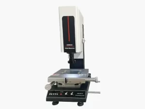
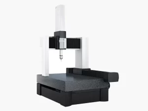
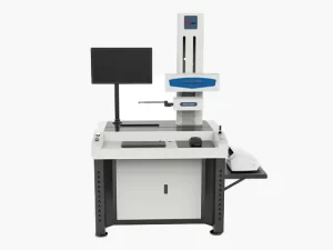
Professional Stylus Surface Profiler – Nanometer-Level Step Height & Surface Roughness Measurement
The Professional Stylus Surface Profiler is a high-precision contact measurement system designed for accurate analysis of step height, surface roughness, and 3D surface topography. Using a diamond stylus that gently traces the sample surface, it captures fine surface variations with exceptional resolution and stability. This ensures highly reliable and repeatable measurement results for demanding industrial and laboratory applications.
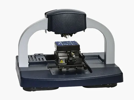
How It Works
The system operates based on a contact-style measurement method. As the stylus moves along the surface, its vertical displacement mirrors the surface contours. This movement is captured as an electrical signal through a measuring bridge, generating an amplitude-modulated output proportional to the vertical displacement. The signal is then amplified, processed through phase-sensitive rectification, and filtered to remove noise and waviness. This ensures that the final output is a clean and stable signal, providing accurate step height and roughness measurements free from external interference and waviness.
Key Applications
- Semiconductor Wafer Metrology: Precise measurement and analysis of semiconductor wafers to ensure high-quality fabrication.
- MEMS and Microstructures: Accurate profiling of MEMS (Micro-Electro-Mechanical Systems) and microstructures for detailed surface measurements.
- Thin Film and Coating Thickness: Evaluation of the thickness and uniformity of thin films and coatings, critical for various manufacturing processes.
- Solar Cell Surface Profiling: Accurate surface measurements for solar cells, optimizing performance and manufacturing quality.
- Precision Optics and Medical Devices: Measurement of precision optics and medical devices to maintain high standards of quality and performance.
Key Features
- Stable Performance: Ensures consistent operation with fast transmission, automatic calibration, and accurate measurement.
- Revolutionary Desktop Design: Achieves a balance of high performance, ease of use, and cost-effectiveness in a compact benchtop setup.
- Compact & Reliable Design: Optimized hardware configuration ensures high testing accuracy, stability, and efficiency.
- Superior Materials & Durability: Crafted with high-quality materials to ensure durability, long service life, and efficient performance.
Equipment Features
- Unrivaled Performance: Step height reproducibility below 4A, with enhanced scanning capabilities.
- Single-Arch Design: Provides breakthrough stability, minimizing ambient noise interference, and enabling a large vertical range with low-force scanning.
- Upgraded Smart Electronics: Reduces noise and enhances measurement accuracy, capable of measuring step heights below 10nm.
- Optimized Hardware Configuration: Reduces data acquisition time by 40%, improving measurement efficiency.
- 64-bit Vision64 Synchronous Software: Accelerates data processing, increasing data analysis speed by 10x.
- Intuitive User Interface: Vision64 software offers a simplified, user-friendly interface for easier setup and analysis.
- Automatic Tip Alignment System: Simplifies probe changes with self-aligning probe assembly, reducing risks during transition.
- Wide Range of Probe Models: Offers various probe sizes and shapes, ensuring compatibility with nearly any application.
- Single Sensor Design: Delivers low-force measurements with a wide scanning range on a single plane.
- High Throughput Testing: Ensures quick, multi-sample testing for precise thin film measurements with superior repeatability.
Technical Parameters
| Measurement Technology | Probe profiling technology |
| Measurement Function | 2D surface profile measurement |
| Optional 3D measurement/ | |
| Sample View | Selectable magnification, 1 to 4mm FOV |
| Probe Sensor | Low inertia sensor (LIS3) |
| Probe Pressure | Using LIS3 sensor: 1 to 15mg |
| Low Force (Optional) | Using N-Lite+ low force sensor: 0.03 to 15mg |
| Probe Options | Probe curvature radius selectable range: 50nm to 25μm; |
| Height-to-diameter ratio (HAR) tips: 10μm*2μm and 200μm*20μm; | |
| Custom tips are available upon request. | |
| Sample X/Y Stage | Manual X-Y translation: 100mm (4 inches) |
| Motorized X-Y translation: 150mm (6 inches) | |
| Sample Rotary Stage | Manual, 360° rotation; |
| Motorized: 360° rotation; | |
| Computer System | 64-bit multi-core line processor, Windows* 7.0; Optional 23-inch flat panel display |
| Software | Vision64 operation and analysis software; |
| Stress measurement software: Cantilever deflection; | |
| Suturing software: 3D scanning imaging software | |
| Vibration Damping Device | Shock damping available |
| Scan Length Range | 55mm (2 inches) |
| Data points per scan | Up to 120,000 data points |
| Maximum sample thickness | 50mm (2 inches) |
| Maximum wafer size | 200mm (8 inches) |
| Step height reproducibility | <4A1σ on a 1μm step |
| Vertical Range | 1mm (0.039 inches) |
| Vertical Resolution | Maximum 1A (at 6.55μm vertical range) |
| Input Voltage | 100 - 240 VAC, 50 - 60Hz |
| Temperature Range | Operating Range 20 to 25°C (68 to 77°F) |
| Humidity Range | ≤80%, Non-condensing |
| System size and weight | 455mm W x 550mm D x 370mm H |
| (179in. W x 22.6in. D x 14.5in. H); | |
| 34 kg (75 lbs); | |
| Attachment: 550mm L x 585mm W x 445mm H (216in. L x 23in. W x 175in. H); | |
| 217 kg (48 lbs) |
Application Cases
- Thin Film Testing – Ensuring High Yields:
In semiconductor manufacturing, Step instrument helps monitor deposition and etching uniformity, thin film stress, and ITO thin film thickness. Its high reproducibility ensures accurate measurement, optimizing etching and deposition for better yields. - Surface Roughness Inspection – Ensuring Performance:
Ideal for assessing surface roughness in precision components across industries like automotive, aerospace, and medical devices. For example, it measures the roughness of orthopedic implant coatings to ensure product quality and adhesion. - Solar Grid Line Analysis – Reducing Manufacturing Costs:
Perfect for measuring the dimensions of conductive silver grid lines on solar panels. Step instrument ensures that silver usage is optimized for better conductivity, contributing to cost-saving in solar panel production. - Microfluidics Technology – Detecting Design and Performance:
Used in MEMS and microfluidics technology for qualification testing. The low-force NLite+ measurement function enables precise detection of vertical steps and roughness on photosensitive materials, ensuring design accuracy and performance.
Get Started with Your Solutions Today!
Whether you're looking for high-performance CNC machines or reliable manual machines, we offer tailored solutions to meet your specific needs.
Contact us today to discuss your requirements and get expert advice. Let us help you optimize your manufacturing processes!
Our Advantages
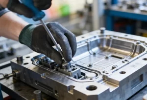
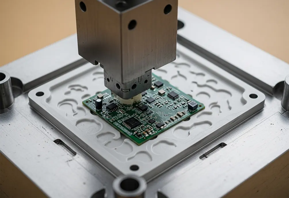
Backed by over 25 years of engineering experience, our team offers comprehensive services—from customized mold design and precision machining to full-scale production—supported by a robust quality assurance system and proactive customer service. Certified under ISO9001, ISO14001, and IATF 16949, we continually strive for excellence in quality, innovation, and customer satisfaction.
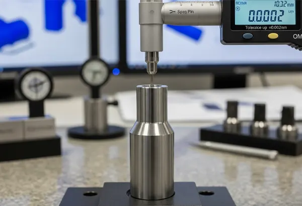
Tolerance Precision Up to ±0.002mm
Selected authentic ingredients 1 piece is equivalent to 5 pieces
Batch processing and customization based on drawings, free sampling.
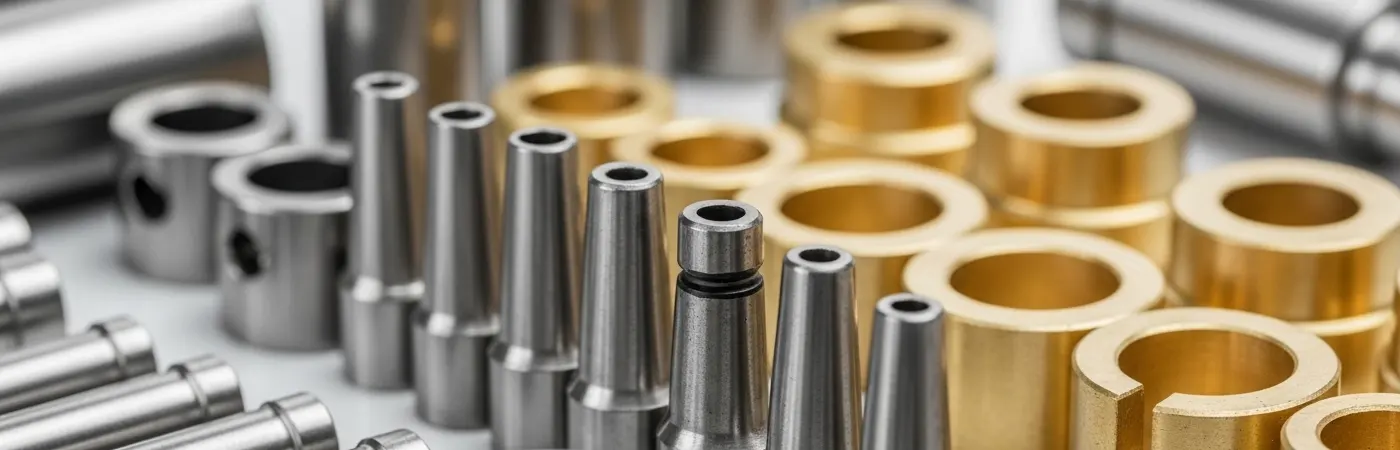
Application Range
The preferred choice across various industries.